
A316J IC - Optocoupler IC - SMD Package
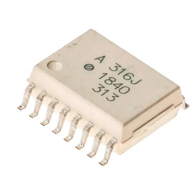
A316J IC - Optocoupler IC - SMD Package
The A316J Optocoupler with Integrated Desaturation (VCE) Detection and Fault Status Feedback makes IGBT VCE fault protection compact, affordable, and easy-to-implement while satisfying worldwide safety and regulatory requirements. The A316J is an easy-to-use, intelligent gate driver which makes IGBT
+ 18% GST (added at checkout)
In stock — 522 units ready
Buying in bulk?
Get volume pricing, GST invoicing and stock availability for larger quantities of this item.
The A316J Optocoupler with Integrated Desaturation (VCE) Detection and Fault Status Feedback makes IGBT VCE fault protection compact, affordable, and easy-to-implement while satisfying worldwide safety and regulatory requirements. The A316J is an easy-to-use, intelligent gate driver which makes IGBT VCE fault protection compact, affordable, and easy-to-implement. Features such as user configurable inputs, integrated VCE detection, under voltage lockout (UVLO), “soft” IGBT turn-off and isolated fault feedback provide maximum design flexibility and circuit protection. Features:- • 2.5 A maximum peak output current • Drive IGBTs up to IC = 150A, VCE = 1200V • Optically isolated, FAULT status feedback • SO-16 package • CMOS/TTL compatible • 500 ns max. switching speeds • “Soft” IGBT turn-off • Integrated fail-safe IGBT protection – Desat (VCE) detection – Under Voltage Lock-Out protection (UVLO) with hysteresis • User configurable: inverting, noninverting, auto-reset, auto-shutdown • Wide operating VCC range: 15 to 30 Volts • -40°C to +100°C operating temperature range • 15 kV/µs min. Common Mode Rejection (CMR) at VCM=1500V • Regulatory approvals: UL, CSA, IEC/EN/DIN EN 60747- 5-5 (1414 V peak Working Voltage) Specification:- Symbol Parameter Min Max Units TS Storage Temperature -55 125 °C TA Operating Temperature -40 100 TJ Output IC Junction Temperature 125 |Io(peak)| Peak Output Current 2.5 A IFAULT Fault Output Current 8 mA VCC1 Positive Input Supply Voltage -0.5 5.5 V VIN+, VIN- and VRESET Input Pin Voltages -0.5 VCC1 (VCC2 - VEE) Total Output Supply Voltage -0.5 35 (VE - VEE) Negative Output Supply Voltage -0.5 15 (VCC2 - VE Positive Output Supply Voltage -0.5 35 - (VE - VEE) Vo(peak) Gate Drive Output Voltage -0.5 VCC2 Related Document:-
You may also need
A316J IC - Optocoupler IC - SMD Package