
CD4015 Dual 4-Stage Shift Register IC DIP-16 Package
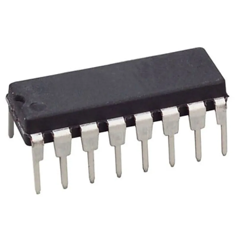
CD4015 Dual 4-Stage Shift Register IC DIP-16 Package
CD4015 consists of two identical, independent, 4-stage serial-input/parallel-output registers. Each register has independent CLOCK and RESET inputs as well as a single serial DATA input. "Q" outputs are available from each of the four stages on both registers. All register stages are D-type, master-
+ 18% GST (added at checkout)
In stock — 1660 units ready
Buying in bulk?
Get volume pricing, GST invoicing and stock availability for larger quantities of this item.
CD4015 consists of two identical, independent, 4-stage serial-input/parallel-output registers. Each register has independent CLOCK and RESET inputs as well as a single serial DATA input. "Q" outputs are available from each of the four stages on both registers. All register stages are D-type, master-slave flip-flops. The logic level present at the DATA input is transferred into the first register stage and shifted over one stage at each positive-going clock transition. Resetting of all stages is accomplished by a high level on the reset line. Register expansion to 8 stages using one CD4015 package, or to more than 8 stages using additional CD4015’s is possible. The CD4015-series types are supplied in 16-lead hermetic dual-in-line ceramic packages (F3A suffix), 16-lead dual-in-line plastic package (E suffix), 16-lead small-outline packages (M, M96, MT, and NSR suffixes), and 16-lead thin shrink small-outline packages (PW and PWR suffixes). Features:- Medium speed operation...12 MHz (typ.) clock rate at V DD – V SS = 10 V Fully static operation 8 master-slave flip-flops plus input and output buffering 100% tested for quiescent current at 20 V 5-V, 10-V, and 15-V parametric ratings Standardized, symmetrical output characteristics Maximum input current of 1 µA at 18 V over full package-temperature range; 100 nA at 18 V and 25°C Noise margin (full package-temperature range) = 1 V at V DD = 5 V 2 V at V DD = 10 V 2.5 V at V DD = 15 V Meets all requirements of JEDEC Tentative Standard No. 13B, "Standard Specifications for Description of ’B’ Series CMOS Devices" Applications: Serial-input/parallel-output data queueing Serial to parallel data conversion General-purpose register Specifications:- Parameter Specification Part number CD4015B Technology Family CD4000 VCC (Min) (V) 3 VCC (Max) (V) 18 Voltage (Nom) (V) 10 F @ nom voltage (Max) (MHz) 8 ICC @ nom voltage (Max) (mA) 0.3 tpd @ nom Voltage (Max (ns) 160 IOL (Max) (mA) 1.5 IOH (Max) (mA) -1.5 3-state output No Rating See Data Sheet Operating temperature range (C) -55 to 125 Related Document:- CD4015 IC Datasheet
You may also need
CD4015 Dual 4-Stage Shift Register IC DIP-16 Package