
CD4099 8 bit Addressable Latch IC DIP-16 Package
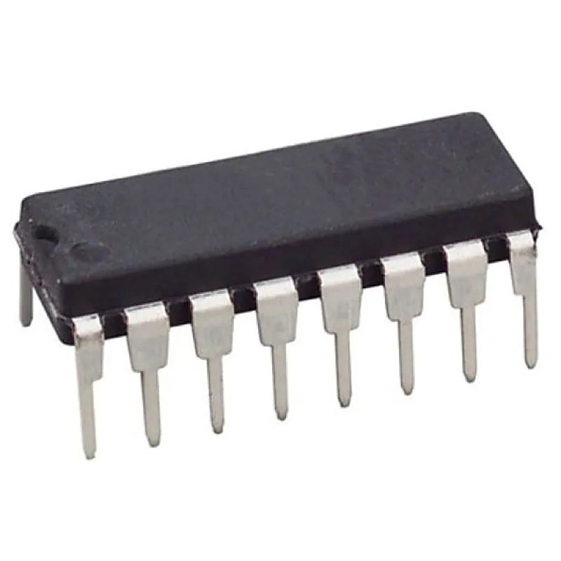
CD4099 8 bit Addressable Latch IC DIP-16 Package
CD4099 8-bit addressable latch is a serial-input, parallel-output storage register that can perform a variety of functions. Data are inputted to a particular bit in the latch when that bit is addressed (by means of input A0, A1, A2) and when WRITE DISABLE is at a low level. When WRITE DISABLE is hig
+ 18% GST (added at checkout)
In stock — 2738 units ready
Buying in bulk?
Get volume pricing, GST invoicing and stock availability for larger quantities of this item.
CD4099 8-bit addressable latch is a serial-input, parallel-output storage register that can perform a variety of functions. Data are inputted to a particular bit in the latch when that bit is addressed (by means of input A0, A1, A2) and when WRITE DISABLE is at a low level. When WRITE DISABLE is high, data entry is inhibited; however, all 8 outputs can be continuously read independent of WRITE DISABLE and address inputs. A master RESET input is available, which resets all bits to a logic "0" level when RESET and WRITE DISABLE are at a high level. When RESET is at a high level, and WRITE RESET is at a low level, the latch acts as a 1-of-8 demultiplexer; the bit that is addressed has an active output which follows the data input, while all unaddressed bits are held to a logic "0" level. The CD4099 types are supplied in 16-lead hermetic dual-in-line ceramic packages (F3A suffix), 16-lead dual-in-line plastic package (E suffix), 16-lead small-outline package (M, M96, MT, and NSR suffixes), and 16-lead thin shrink small-outline packages (PW and PWR suffixes). Features:- Serial data input Active parallel output Storage register capability Master clear Can function as demultiplexer Standardized, symmetrical output characteristics 100% tested for quiescent current at 20 V Maximum input current of 1 uA at 18 V over full package-temperature range; 100 nA at 18 V and 25°C Noise margin (full package-temperature range) = 1 V at V DD = 5 V 2 V at V DD = 10 V 2.5 V at V DD = 15 V 5-V, 10-V, and 15-V parametric ratings Meets all requirements of JEDEC Tentative Standard No. 13B, "Standard Specifications for Description of ’B’ Series CMOS Devices" Applications: Multi-line decoders A/D converters Specifications:- Parameter Specification Part number CD4099B Technology Family CD4000 VCC (Min) (V) 3 VCC (Max) (V) 18 Bits (#) 8 Voltage (Nom) (V) 10 F @ nom voltage (Max) (MHz) 8 ICC @ nom voltage (Max) (mA) 0.3 tpd @ nom Voltage (Max) (ns) 150 IOL (Max) (mA) 1.5 IOH (Max) (mA) -1.5 3-state output No Operating temperature range (C) -55 to 125 Related Document:- CD4099 IC Datasheet
You may also need
CD4099 8 bit Addressable Latch IC DIP-16 Package